Allion Labs
After reading many technical terms from the previous article, let us explore comprehensively how Allion assists customers in saving time and cost to be more competitive on products by visiting the factory.
Common Issue 1: The Chip Pin is Warped
VP6116RYM HF (DC:2145) The material has poor soldering on the edge of the pin, and the defective rate is 4/605=6611DPPM (defective parts per million)
Upon checking on site, the pin is confirmed warped as the edge of it is in contact with the tin without being soldered.
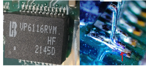
Upon analysis of the defective sample, there is sticky tin on the pin from the product. We can see that the upturned pin is right on the edge of the 0.1 mm mark after the test with 40 times optical analyzer.

Root Cause:
- Projection:
1) The projection uses 40 times optical analyzer to assess the flatness of the product. The standard of flatness is below 0.1 mm, and it is strictly controlled to be below 0.8 mm. (as shown in Figure 3)
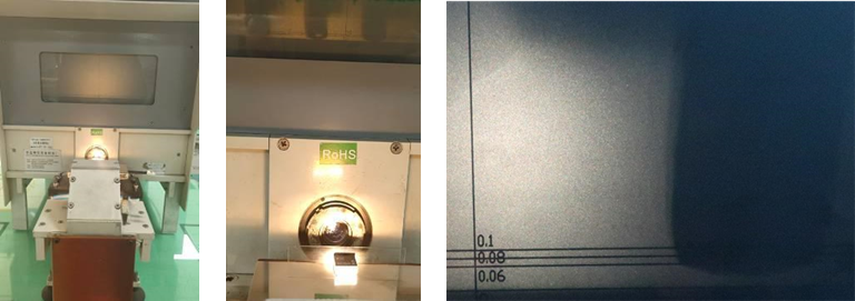
Figure 3: The projection Pin is below 0.08 mm
2) The product is placed on the platform when inspected with projection throughout the on-site inspection. The pin is thoroughly checked on the platform with three test lines on it. The pin is set right within three lines (as shown in Figure 4), and the distance of lines is minimal in between; hence judgment error occurs due to visual fatigue of production line workers working for a long time. The pin on the edge of the 0.1 mm line cannot be removed.

Figure 4: PIN The pin is set to be within three lines
- FQC Product Inspection Station: The flatness test is performed on products that exceed a strict specification, and nothing is detected.
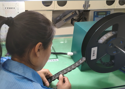
- Tape inspection for post-packaging: A complete inspection of appearance is conducted after packaging (as shown in Figure 5 ). The slightly upturned pin in the tape is difficult to be removed by visual inspection. Thus it is shipped to the customers.
Solution:
Modify the standard on the projector from three lines to one (keep a 0.08 mm mark) to avoid misjudgment.

Person in charge: Lin Hsiao-Rong (林小蓉)/Hsieh Ming-Jun(謝明君), Date of execution: 2022.02.25
Based on the modification of the standard line on the projector, 2100 pcs of products from the same organization are checked and inspected by FQC. Production and delivery will be followed up if there is no defect. According to the sales report, there is no RMA claim on products in the batch inspected by QC standards.
Common Issue 2: Component Displacement
Spec: The PAD/PIN of the component is misaligned with the PAD of the PCB, and it exceeds 1/2 of the part width
Defective Rate: 3/726=4132DPPM
Sign of Defects:

Root Cause:
- The flux in solder paste will deteriorate, resulting in poor soldering if the period of it exceeds the limit.
- The component shifts during transportation due to low viscosity of the solder paste.
- The solder paste contains a large amount of flux, which causes the component to displace during the reflow process.
- The components are displaced due to vibration in transportation or incorrect handling after printing and placement.
- The components are shifted as the suction nozzle is not adjusted correctly with insufficient pressure during the placement process.
- The mechanical issue of the placement machine causes the components to be displaced.
Solution:
- Calibrating the alignment strictly to ensure the accuracy of component placement.
- Use high quality and adherence of solder paste to enhance the SMT pressure of components and bonding force.
- Select proper solder paste with a decent amount of flux content to avoid collapse.
- Adjust the pressure with a suction nozzle, and the placement should be above 400mmHG.
Common Issue 3: The Pad with Tin
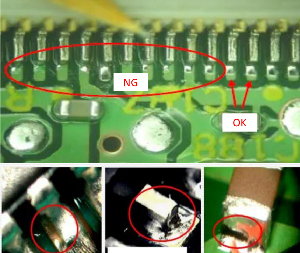
Spec: The pin of parts, PCB, and PAD is welded with tin, but the standard of the tin amount is not met.
Defective Rate: 2/425=4705 DPPM
Sign of Defects:
Root Cause:
- If the printing process stops for a long time, the flux at the opening of the stencil will harden and blocks the opening spot.
- Insufficient stirring of the solder paste causes bad rolling; deterioration of the solder paste causes high viscosity and less adhesion.
- Uneven scraper.
Solution:
- A thorough cleaning of the stencil must be performed.
- Pay attention to the opening and use time on solder paste and stir.
- Check the scrape periodically or before the initiation of production.
Common Issue 4: RAM Slot Bridging
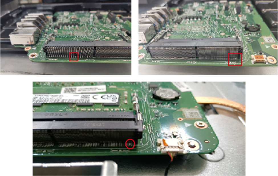
Defective Rate: 3/726=4132DPPM
Sign of Defects:
Root Cause:
- Based on observation, the defect is not concentrated but anywhere in the RAM slot. Also, the bridging is spotted at the curving part of the pin.
- It is possible to find bridging in the reflow process by tracing the SPI log.
- The amount of solder paste is found to be high (compared with previous ones) by checking the production record.
- Based on the data, the opening of the stencil is bigger compared to previous ones, hence resulting in a huge area of the pad being covered by the tin. (the tin is 0.1mm2 more per piece)
Solution:
Modify the stencil parameter by changing L*W=2mm*0.238 mm to L*W=1.85mm*0.22mm. Change the tin area from 0.0619 mm2 to 0.0529 mm2. Refer to the parameters below.
According to the above case, there are still issues that cannot be spotted right away even though the factory has SMT QC staff and the production efficiency and quality are lower. However, with Allion’s SMT service, most of the issues can be found immediately.
Besides the above SMT testing objects, Allion also offers tests for your customized products from IQC (Incoming Quality Control) to IPQC (In Process Quality Control), even QQC before dispatching. Please do not hesitate to contact Allion should you need further factory tests.


